


Engineering Support & Customer Service
FR4 PCB Prototype
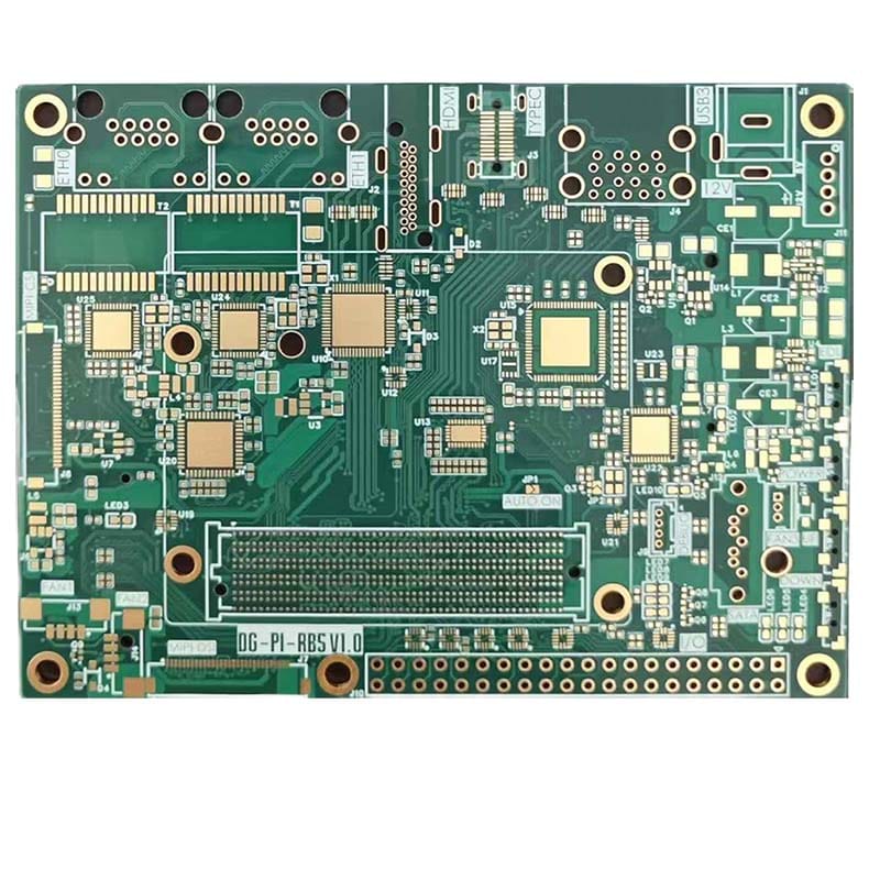
Muti-Layer PCB
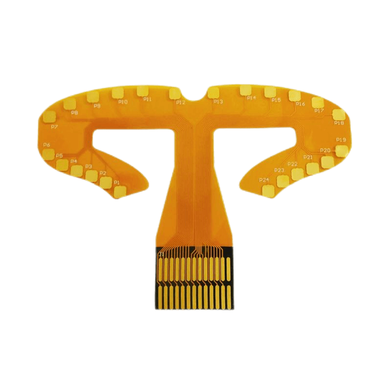
Flexible PCB
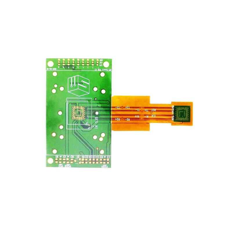
Rigid-Flex PCB

Aluminum PCB

High Copper PCB

HDI PCB
High Frequency PCB
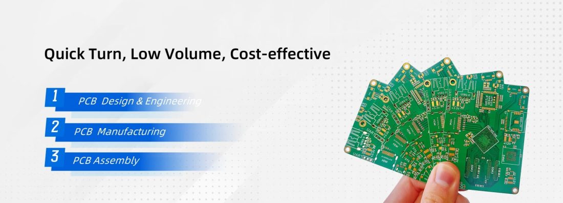
PCB Capabilities
Rigid PCB Manufacturing Capabilities
| Features | Capabilty | Description |
| Layer | 2/4/6/8/10/12/14/16/18/20.../32 layers PCB | The number of copper layers in the PCB |
| Impedance Tolerance | ±10% | |
| Material | FR-4 | |
| Aluminum-Core | One layer Aluminum-core PCB | |
| Copper-Core | One layer copper-core PCB with direct heatsink contacts to core(≥1 x 1 mm) | |
| RF PCB | 10z copper, 2-layer RF PCB with Rogers and PTFE core | |
| FR-4 Dielectric Constants | 4.5(2-Layer PCB) | 7628 Prepreg 4.4 3313 Perpreg 4.1 2116 Perpreg 4.16 |
| Max. Board Dimensions | FR4 PCB: 600×600 mm Rogers/PTFE Teflon PCB: 550×400mm Aluminum PCB: 600×500 mm Copper PCB: 480×280mm | These limits apply to PCBs with thickness ≥0.8mm. The thinner FR4 PCBs are 500×600 mm maximum. 2-layer FR4 PCBs can reach a maximum size of 1000x660mm |
| Min. Board Dimensions | Regular: 3×3mm. Castellated/Plated Edges: 10×10mm. | These limits apply to PCBs with thickness ≥0.6mm. Manual review required for thinner PCBs. Panelization is recommended for small-sized boards. |
| Dimension Tolerance | ±0.1mm | ±0.1mm(Precsion) and ±02mm(Regular) for CNC routing, and ±0.4mm for V-Cut |
| Thickness | 0.4-4.5mm | Thickness for FR4 are:0.4/D.6/0.8/1.DV1.2/1.6/2.0 mm (2.5mm and above are for 12+layer PCBs only) |
| Thickness Tolerance (Thickness≥1.0mm) | ±10% | e.g. For the 1.6mm board thickness,the finished board thickness ranges from 1.44mm(T-1.6×10%) to 1.76mm(T+1.6×10%) |
| Thickness Tolerance (Thickness<1.0mm) | ±0.1mm | e.g. For the D.8mm board thickness, the finished board thickness ranges from 0.7mm(T-0.1) to 0.9mm(T+0.1) |
| Finished Outer Layer Copper | 1oz/2oz(35um/70um) | Finished copper weight of outer layer is 1oz or 2oz. (Not including the heavy copper PCB) |
| Finished Inner Layer Copper | 0.5oz/1oz/2oz(17.5um/35uml 70um) | Finished copper weight of inner layer is 0.5oz by default. |
| Soldermask | Colors: Green, Purple, Red, Yellow, Blue, White, and Black. | |
| Surface Finish | HASL(leaded/lead-free), ENIG, OSP(copper core boards only) | FR4 PCB has all three finishes available, 6+layers and RF boards only have ENIG. Aluminium core PCBs only have HASL. Copper core PCBs only have OSP. |
Drilling
| Features | Capabilty | Descriptlion |
| Drill Diameter | 1-layer:0.3-6.3mm 2-layer:0.15-6.3mm Multilayer:0.15-6.3mm | Holes with diameter≥6.3mm are CNC routed from a smaller drilled hole. Min. drill diameter for 2-or more-layer PCBs is 0.15mm(more costly) Min. drill diameter for aluminum-core PCBs is 0.65mm Min. drill diameter for copper-core PCBs is 1.0mm |
| Hole size Tolerance(Plated) | Through-holes: +0.13/-0.008mm Press-fit holes: ±0.05mm(multilayer ENIG boards only-mention the specific holes in PCB Remark) | e.g. for the 0.6mm hole size, the finished hole size between 0.52mm to 0.73mm is acceptable. |
| Hole size Tolerance(Non-Plated) | ±0.2mm | e.g. for the 1.00mm Non-Plated hole, the finished hole size between 0.80mm to 1.20mm is acceptable. |
| Average Hole Plating Thickness | 18μm | |
| Blind/Buried Vias | supported | |
| Min. Via hole size/diameter | 0.15mm/0.25mm | 1-layer(NPTH only): 0.3mm hole size/0.5mm via diameter 2-layer 0.15mm hole size/0.25mm via diameter Mutilayer 0.15mm hole size/0.25mm via diameter |
| Min. Non-plated holes | 0.50mm | Please draw NPTHs in the mechanical layer or keep out layer. |
| Min. Plated Slots | 0.5mm | The minimum plated slot width is 0.5mm,which is drawn with a pad. |
| Min. Non-Plated Slots | 1.0mm | The minimum Non-Plated Slot Width is 1.0mm, please draw the slot outline in the mechanical layer(GM1 or GKO) |
| Via Hole-to-Hole Spacing | 0.2mm | |
| Pad Hole-to-Hole Spacing | 0.45mm | |
| Min. Castellated Holes | 0.5mm | Castellated holes are metalized half-holes on PCB edges, commonly used on daughter boards to be soldered onto carrier PCBs. ①Hole diameter(Φ): ≥0.5mm ②Hole to board edge(L): ≥1mm ③Hole to hole(D): ≥0.5mm ④Min. PCB size: 10×10 mm ⑤Min. PCB thicknes: 0.6mm |
| Plated Edges | 10x10mm | Plated edges are copper-plated and ENIG treated. HASLis not supported. ①Min.PCB size:10×10mm ②Min.PCB thickness:0.6mm ③At least 3 breaks (more for larger PCBs) in the edge plating are required for support tab connections |
| Blind Slot | ①Blind slot width (W): ≥1.0mm ②Blind slot depth (D): ≥0.2mm ③Blind slot annular width (A): ≥0.3mm(The pad width of PTH blind slots) ④Safety distance(S): ≥0.2mm (The distance from NPTH blind sots to pad/traces/copper plane) ⑤Blind slot remaining thickness (R): ≥0.2mm(The distance from the bottom of the blind slot to the nearest inner copper layer/surface substrate) ⑥Supports 2-32 layer FR4 boards with a thickness of ≥0.8mm |
Traces
| Features | Capabilty | Descriptlion |
| Min. track width and spacing(1oz) | 0.10/0.10 mm(4/4mil) | One and two layer: 0.10/0.10 mm(4/4mil) Multilayer: 0.09/0.09 mm(3.5/3.5mil). 3mil is aceptable in BGA fan-outs. |
| Min.track width and spacing (2oz) | 0.16/0.16mm(6.5/6.5mil) | 2-layer: 0.16/0.16mm(6.5/6.5mil) Multilayer.0.16/0.20 mm(6.5/8mil) |
| Track width tolerance | 20% | eg. For a 0.1 mm track, the finished track width ranges from 0.08and 0.12mm. |
| PTH annular ring | ≥0.2Dmm | Double-layer: 1 oz: Recommended 0.25mm or above; absolute minimum 0.18mm 2oz: 0.254 mm or above Multilayer: 1oz: Recommended 0.20mm or above; absolute minimum 0.15mm 2oz: 0.254 mm or above |
| NPTH pad annular ring | ≥0.45mm | Recommended 0.45mm or more. This is to allow a 0.2mm ring of copper to be removed around the hole for the sealing film to attach. Pad sizes smaller than the recommended value can result in the annular ring being very thin or completely missing. |
| Ball Grid Array | 0.25mm | ①BGA pad diameter ≥025mm ②BGA pad to trace clearance ≥0.1 mm(min.0.09 mm for multilayer boards) ③Vias can be placed within BGA pads using filled and plated-over vias |
| Trace coils | 0.15/0.15mm | Minimum trace width/clearance: 0.15/0.15mm, when traces are covered by solder mask(1oz). Minimum trace width/clearance: 0.25/0.25mm, when traces are NOT covered by solder mask(1oz). ENIG only(high risk of short circuit with HASL) |
| Hatched grid width and spacing | 0.25mm | |
| Same-net track spacing | 0.25mm | |
| Inner layer via hole to copper clearance | 0.2mm | |
| Inner layer PTH pad hole to copper clearance | 0.3mm | |
| Pad to track clearance | 0.1mm | Min. 0.1 mm(stay wellabove if possible). Min.0.09mm locally for BGA pads |
| SMD pad to pad clearance (different nets) | 0.15mm | More details of SMD pad spacing: SMD Components Minimum Spacing |
| Via hole to Track | 0.2mm | |
| PTH to Track | 0.28mm | 0.35mm is recommended, minimum 0.28mm |
| NPTH to Track | 0.2mm |
Flexible PCB Manufacturing Capabilities
| Features | Descriptlion | Capabilty |
| Layer | One layer,two layers | The number of copper layers in the FPC |
| FPC Stack-Up | Single-Sided | FPC with copper and coverlay on the same one side only. Inner PI thickness: 25μm |
| Double-Sided | FPC with copper on both sides. Inner PI thickness: 25μm | |
| Dimensions | Maximum Dimensions | Regular: 234×490mm |
| Minimum Dimensions | No limit, but the whole dimension smaller than 20×20mm is the best panelised | |
| FPC Finished Thickness | Single-sided: 0.07/0.11mm Double-sided: 0.11/0.12/0.2mm | |
| Outer Layer Copper Weight | Single-sided 18μm(0.5 oz), 35 μm(1oz) Double-sided:12μm(0.33 oz), 18μm(0.50z),35μm(1oz) | |
| Type of Process | Dry film process with LDI(laser direct image) exposure technology | |
| Surface Finish | ENIG Thickness: 1u"/2u" | |
| Thickness with Stiffener | Thickness with Stiffener is FPC Thickness + Stiffener Thickness | |
| FPC Thickness Tolerance | ±0.05mm | |
| Holes | Hole Diameter | 0.15-6.5mm |
| Diameter Tolerance | ±0.08 mm | |
| Minimum Plated Slot | 0.50mm | |
| Minimum Non-Plated Slot | Not limited | |
| Castellated Holes | Castellated holes are plated half-holes on the edge of an FPC. Most often used for press-soldered connectors. ①Castellated hole diameter. ≥0.3mm ②Castellated hole to board edge: ≥0.5mm ③Castellated hole to hole: ≥0.4 mm | |
| Min. Via hole size/diameter | 0.15mm (Via hole size)/0.35mm(Via diameter) ①Annular ring: 0.1 mm minimum, 0.125mm recommended ②Recommended via size: 0.3mm inner, 0.55mm outer | |
| Traces | Annular Ring for PTH | ≥0.25mm recommended, absolute limit 0.18mm |
| Minimum Trace Width/Spacing(1oz) | ①12 μm(0.33 oz)copper. 3/3mil (absolute limit 2/2 mil) ②18μm(0.5 oz)copper: 3.5/3.5mil ③35 μm(1oz)copper: 4/4mil These are regular capabilifies. Contact customer support for custom capability requirements. | |
| Trace Width Tolerance | ±20% | |
| Pad-to-Trace Clearance | ①Via ring to trace: ≥0.1mm ②Exposed pad to trace: ≥0.15mm | |
| NPTH to Copper Clearance | ≥0.20 mm | |
| Ball Grid Array | ①BGA pad diameter: ≥0.25mm ②BGA pad to trace clearance: ≥0.2mm | |
| Coverlay/ Soldermask | Coverlay Color | Yellow/Black/White |
| Coverlay Opening | Coverlay expansion(one-sided): 0.1 mm Coverlay opening to trace clearance: ≥0.15mm | |
| Ma covering | Recommended to keep coverlay over vias | |
| Coverlay Thickness | ①PI:12.5μm, glue:15μm(on 12/18μm copper) ②PI:25μm, glue:25μm(on 35μm copper) | |
| Minimum solder bridge width | 0.5mm minimum, i.e. solder bridge narrower than 0.5mm will be removed. Contact customer support for any non-standard requirements. | |
| Silkscreen | Character Height | ≥1mm(More in case of complex patterns or knock-out tex) |
| Character Line Width | ≥0.15mm(Narrower lines do not print well) | |
| Character to Pad Clearance | ≥0.15mm(Any silkscreen closer to a pad than this will be clipped) | |
| FPC Outline | Laser Outline | ①Copper to board edge ≥0.3mm ②Copper to slots ≥0.3mm ③Outline tolerance: ±0.1 mm(±0.05mm upon request) |
| Gold Finger Pad to Board Edge Clearance | 0.2mm. Gold fingers will be cut back if exceeding this clearance to avoid damage during laser cutting the outline. Castellated pads are exempt from this clearance. | |
| Panels (See FPC Panel Design Guide) | ①Spacing between boards is commonly 2mm.For boards with metal stiffeners use 3mm instead. ②Handling edges of width 5mm required on all four sides. Copper pour is required on these edges, with 1mm clearance around fiducials and 0.5mm clearance around tooling holes. ③Fiducials: 1mm; tooling holes: 2mm; Fiducial centre to board edge: 3.85mm Add four fiducials with one offset by 5mm or more. ④Support tab width: 0.7-1.0mm ⑤Maximum panel size: 230×480 mm | |
| FPC Stiffeners | PI Stiffener | Thickness options: 0.1mm, 0.15mm, 0.20 mm, 0.225mm, 0.25mm |
| FR4 Stiffener | Thickness options: 0.1mm,0.2mm | |
| Stainless Steel Stifener | Thickness options: 0.1mm, 0.2mm, 0.3mm | |
| 3M Tape | 3M9077 (0.05mm thick, heat-resistant) 3M468(0.13mm thick, not heat-resistant) | |
| EM Shielding Film | 18μm thick, black Helps lower EMC. The recommended practice is to add soldemask openings over edge guard rails to electrically connect them to the shield films. | |
| Design Considerations | Impedance Calculation | Core polyimide er.3.3 Coverlay er.2.9 Core polyimide thickness:25μm |
| Other Design Constraints | Same requirements as rigid PCBs in terms of holes, traces, soldermask, and silkscreen. |
FAQs
A PCB schematic diagram is a visual representation of an electronic circuit, showing how components like resistors, capacitors, and ICs are connected to form the circuit. It serves as a blueprint for designing the PCB layout and guides engineers during the manufacturing process.
A PCB stackup is the arrangement of copper layers and insulating materials in a printed circuit board. It defines how signals, power, and ground layers are structured, affecting the board's performance, EMI, and manufacturability—especially in multilayer PCBs.
HASL (Hot Air Solder Leveling): A cost-effective PCB surface finish using molten solder. It's good for larger components but not ideal for fine-pitch or high-density boards. ENIG (Electroless Nickel Immersion Gold): A flat, smooth, and highly reliable finish, ideal for fine-pitch, BGA, and high-end PCBs. Offers better corrosion resistance and shelf life.
1.Automated Optical Inspection (AOI) – Checks for surface defects using cameras. 2.In-Circuit Testing (ICT) – Tests electrical performance of components on the board. 3.Flying Probe Test – Uses moving probes to test points on low- to mid-volume boards. 4.Functional Testing (FCT) – Simulates real-world operation to verify full functionality. 5.X-Ray Inspection (AXI) – Inspects hidden solder joints (like BGA) and inner layers. 6.Burn-In Testing – Stresses the PCB to identify early-life failures. 7.Visual Inspection – Manual check for surface defects, often a final quality step.

