
Engineering Support & Customer Service

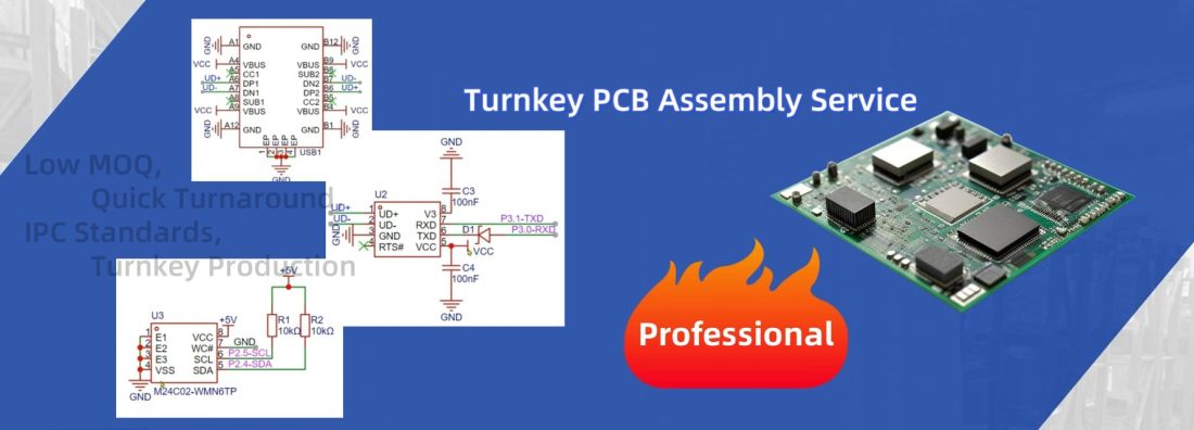
Low MOQ | Quick Turnaround | IPC Standards | Turnkey PCB Production
PCB Assembly Services for Prototypes and Scalable Production
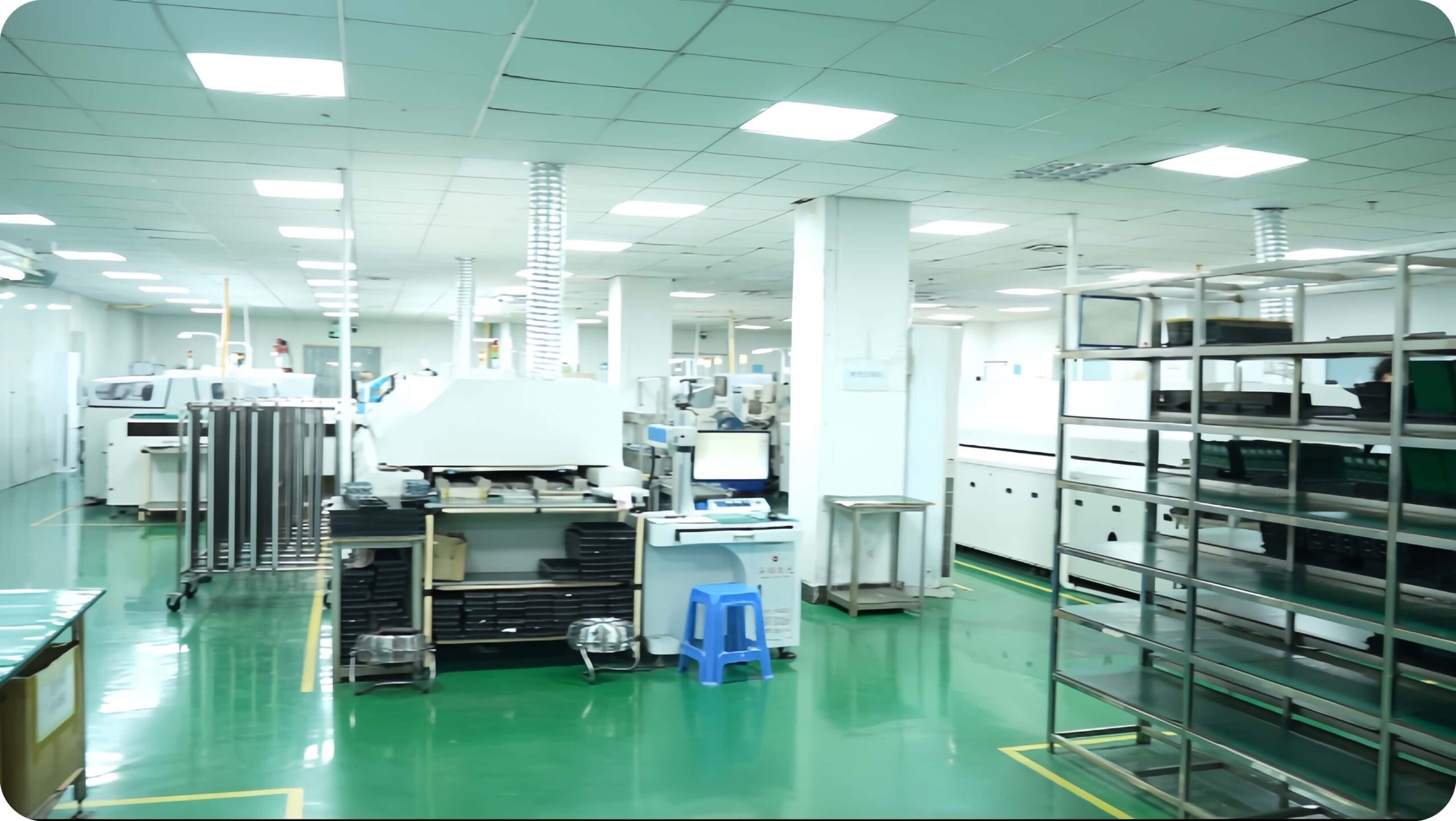
We provide PCB assembly services designed to support projects from early prototyping through low and medium volume production, with scalable processes to support volume ramp-up.
Our focus is on engineering support, process control, and risk reduction to ensure a smooth transition from design to manufacturing.
Assembly Solutions for Different Project Stages
Prototype & Engineering Builds
Fast-turn PCBA
BOM check & DFM feedback
Ideal for validation and testing
Low to Medium Volume Production
Stable processes
Consistent quality
Flexible scheduling
Scalable Production Support
Process optimization
Documentation & control
Support for volume ramp-up
Component Sourcing for PCB Assembly
Streamline your production with our trusted PCB component sourcing services. We work with verified global suppliers to ensure genuine, high-quality parts at competitive prices. Avoid delays, shortages, and counterfeit risks—let us handle the sourcing so you can focus on design and innovation.

S-Chip

Axial

BGA

ACE

CONN_SMD

CONN_THD

Dip

LCC

Melf

Mld

Cry_SMD

Cry_THD

QFN

Radial

SOD


BOM & CPL File Support for PCB Assembly
Our assembly processes are designed to support both early-stage builds and long-term production programs, with scalable capacity and controlled processes to meet growing demand.
PCB Capabilities
PCB Assembly Capabilities
| Features | Standard PCBA | ||
| Assembly Types | Single & double sided placement(SMT/Thru-hole) | ||
| PCB Layer | 1-32 layers | ||
| Thickness | No limit | ||
| Dimension | Single PCB Size: 70x70mm-460x500mm PCB Panel Size: 70x70mm-250×250mm | ||
| Order Volume | 2-80000 pcs | ||
| Surface Finish | No limit | ||
| PCB Color | No limit | ||
| Delivery Format | Single PCB, Panel with mouse bites, Panel with V-cut | ||
| Layer Stackup | All stack-up | ||
| Gold Fingers/Castellated H oles/Edge Plating | Support | ||
| Edge Rails | Necessary | ||
| Fiducials | Necessary | ||
| Minimum Package | 201 | ||
| Minimum IC Pin Spacing | 0.35mm | ||
| Minimum BGASpacing | 0.35mm(center to center) | ||
| Reflow temperature | 240+/-5℃ | ||
| SPI | Yes | ||
| AOI | Yes | ||
| Visual Inspection | Yes | ||
| X-ray Inspection | Yes (only for certain parts, such as BGA) | ||
| Build time | ≥4 days |
PCB Specs for Economic PCB Assembly
| Layer | Thickness(mm) | Color | Surface Finish |
| 2L | 0.8 | Green | HASL-Leaded/Lead free |
| 1 | Green/Black | HASL-Leaded/Lead free | |
| 1.2 | Green/Black | HASL-Leaded/Lead free | |
| 1.6 | Green | HASL-Leaded/Lead free/ENIG | |
| 1.6 | Black | HASL-Leaded/Lead free | |
| 1.6 | Blue/RedWhite/Purple | HASL-Leaded/Lead free | |
| 4L | 1 | Green | HASL-Leaded/Lead free |
| 1.2 | Green | HASL-Leaded/Lead free | |
| 1.6 | Green | HASL-Leaded/Lead free/ENIG | |
| 6L | 1.6 | Green | ENIG |
